Introduction
Latches and flip-flops play important roles in the building of digital CMOS circuits. Timing elements such as flip-flops and latches in addition to the building blocks of any clocking system, form the most important components in synchronous VLSI system. Moreover, the key signal in all synchronous systems is the apparent clock and clock signal is normally heavily loaded by all the latches and flip-flops in the chip, and by the clock distribution network that covers the whole chip. Lastly, although the activity ratio of the clock signal is unity, the interconnection length of the clock trees has been increasing radically. The design trend is thus to increase the pipeline stages for high throughput, and this has prompted the increased in the number of latches and flip-flops in a chip.
Latches and flip-flops must ensure low latency because of the tight timing budget in GHz operations. Power requirement is also becoming increasingly important since the power consumption increases linearly with clock frequency while the power budget of high-performance portable digital systems is severely limited. In power constrained systems, the power efficiency of latches and flip-flops is therefore pivotal. As a result, it is important to trim down the power consumptions in the clock trees, latches and flip-flops.
Circuit Operation
TRANSMISSION-GATE BASED FLIP-FLOP
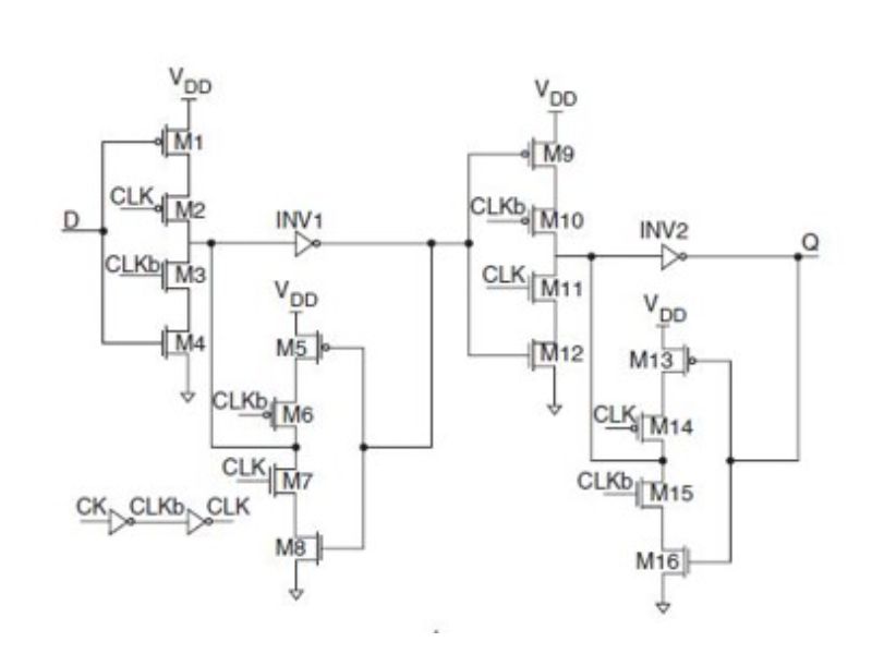
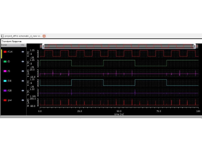
This is a positive level-sensitive latch (transparent when CLK = 1 and in hold for CLK = 0).When the CLK is HIGH, TG1 turns on and D input is passed to the output. Otherwise the latch will go into hold mode (CLK = LOW). The TGATE latch is commonly used as a basis for flip-flop design in standard CMOS cell libraries. However, the TGATE latch consumes relatively high clock power and this would imply a considerable number of clocked transistors in heavily pipelined circuits, which is another drawback of such a design.
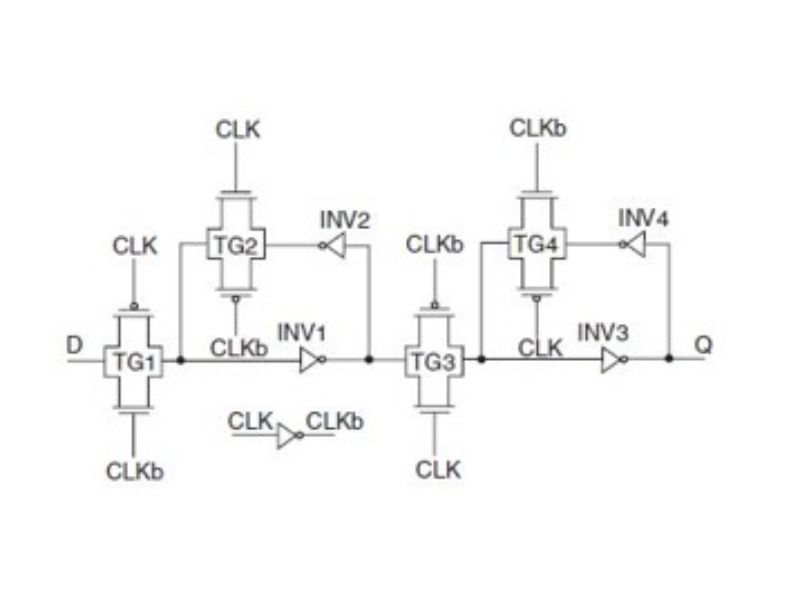
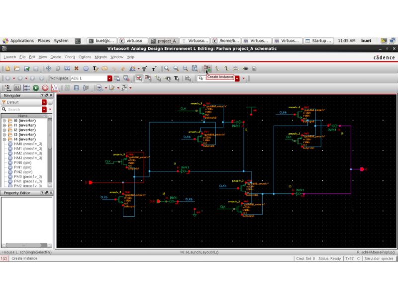
Schematic
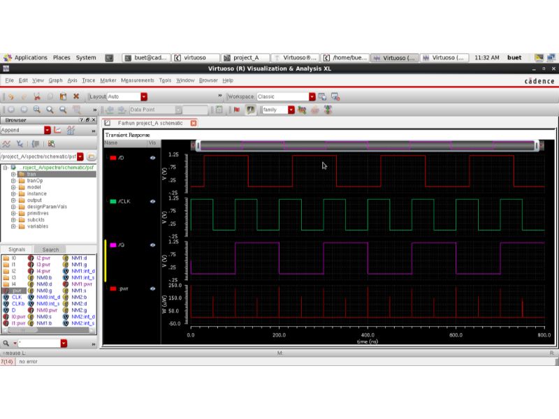
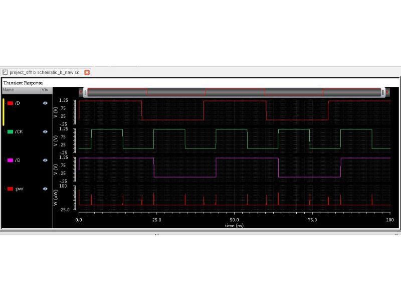
Output
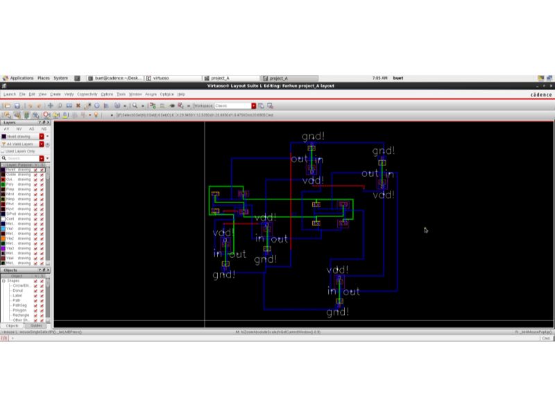
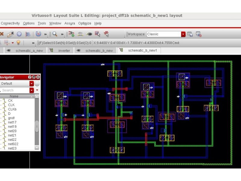
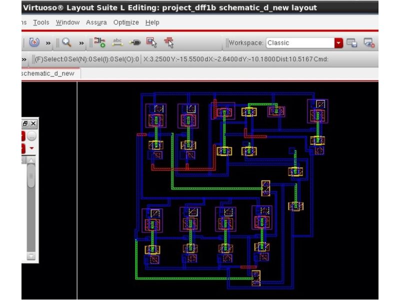
Layout
MODIFIED C2MOS FLIP-FLOP:
Because of the involvement of clocked inverters , this structure is called a C2MOS latch . The dynamic C2MOS latch is modified to a pseudo-static C2MOS latch by adding a C2MOS feedback at the output. It has a small clock load that is made possible by the local clock buffering, and a low-power feedback holding circuit, to secure a fully static operation. However, owing to the two PMOS transistors that are put in series at the pull-up section, the circuit suffers slow rise time.
Layout
Output
Layout
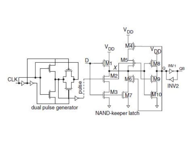
NAND-KEPEER PULSED FLIP-FLOP
The basic difference between NAND keeper latch and flip-flop is that, the CLK input is replaced with an edge-triggered pulse train. When the input D is at a logic LOW value during the HIGH clock level, the internal node X will be a HIGH logic value, driving output Q to a LOW. Alternatively if the input D is HIGH at the positive clock level, node X will transit to a LOW value and the output Q will be pulled to HIGH.
Schematic
Output
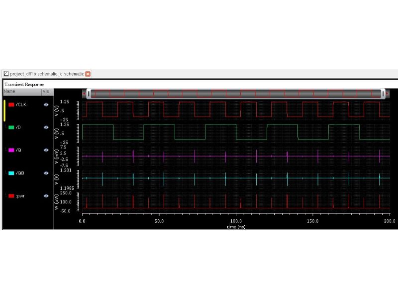
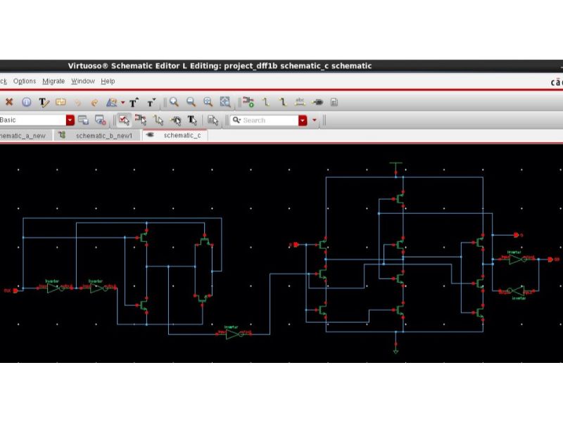
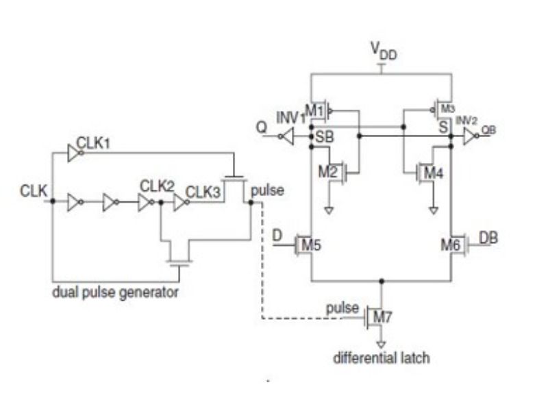
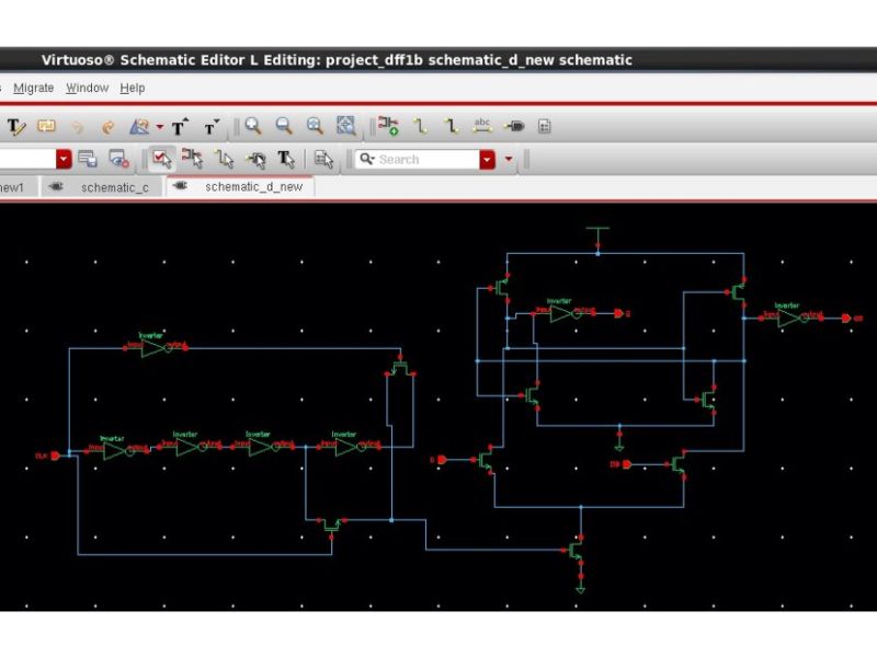
STATIC DIFFERENTIAL PULSED FLIP-FLOP
It is a positive latch as that changes of the input value can be transmitted to the output when the CLK is HIGH. When the input D is HIGH at the positive clock level, output Q and QB will be at HIGH and LOW, respectively. This circuit employs cross-coupled inverters (M1, M2, M3 and M4) to keep the output during clock LOW level.
Schematic
Output
Layout
Comparison Between Flip-Flops
| Flip-Flops | Uses | Drawbacks |
|---|---|---|
| Tgate | Used as a basis for flip-flop design in standard CMOS cell libraries | Consumes relatively high clock power |
| C2MOS | Secure static operation | Suffers slow rise time |
| NAND | Storage devices | The capacitive load will be larger |
| DIFF LATCH | Ecross-coupled inverters to keep the output during clock LOW level | Double input and output capacitive load |
We have analyzed different latches and flip-flops. The classic transmission-gate-based master-slave flip-flop is realized by using two complementary gate latches operating on complementary clocks. The second topology, flip-flop constructed using C2MOS latch. Then both NAND-keeper flip-flop & static differential pulsed flip-flop are dual edge-triggered flip-flop designs since they employ external dual pulse generator. Total power of TGATE flip-flop is comparatively lower than other circuits. So, it will show high performances in various applications. The differences among these four circuits are: First two circuits don’t have external dual pulse generator, we used CLK only as multiple times input and on the other hand second two circuits have external dual pulse generator to which the CLK passes through .